
Big Fund III’s 300B Yuan Allocation: Equipment, Materials, and HBM Breakdown
China’s third national semiconductor investment vehicle—commonly referred to as “Big Fund III”—marks a new phase in the country’s effort to build a more self‑sufficient and globally competitive chip ecosystem. With a planned war chest on the order of 300 billion yuan, the fund is widely expected to pivot from simply backing wafer capacity toward deeper, more targeted investments in equipment, materials, and memory technologies such as high‑bandwidth memory (HBM).
This article interprets that 300B yuan mandate through a strategic lens: what Big Fund III is likely trying to accomplish, how a plausible allocation across equipment, materials, and memory/HBM might look, what it means for China’s semiconductor trajectory, and how international players should respond.
From capacity to capability: what’s different about Big Fund III
The first two iterations of China’s “Big Fund” focused heavily on scaling domestic wafer capacity, backing foundries, IDMs, and related infrastructure to ensure that China could produce more chips at home and reduce its dependence on imports. Over time, this helped catalyze new fabs, expand mature‑node capacity, and support leading domestic foundries. But the global environment has changed: export controls on advanced equipment, rising geopolitical tensions, and the growing importance of advanced packaging and memory have exposed bottlenecks beyond mere wafer count.
Big Fund III is widely understood to be more capability‑oriented. Instead of just asking “how many wafers can we produce?” the focus shifts to “how much of the stack—equipment, materials, memory, packaging—can we own or control domestically?” A 300B yuan envelope is large enough to seed substantial progress in several of these layers, but not enough to solve everything at once. That makes allocation strategy crucial.
Strategic priorities behind the 300B yuan envelope
Although formal breakdowns are not public in detail, it is reasonable to assume that Big Fund III’s capital must balance three broad priorities:
1. Semiconductor equipment. Tooling remains a central choke point in global chip production. Lithography, etch, deposition, metrology, cleaning, and advanced packaging tools are areas where foreign vendors—particularly from Europe, Japan, and the United States—still dominate. Export controls on certain advanced tools further elevate the need for domestic alternatives. Big Fund III is therefore likely to direct a meaningful share of capital toward strengthening homegrown equipment makers, with emphases on segments that are not restricted or that can be indigenized over time.
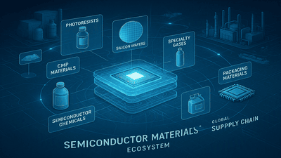
2. Materials and consumables. High‑purity gases, specialty chemicals, photoresists, advanced substrates, and wafer materials are all essential inputs. While China has a strong base in some chemical and materials sectors, the highest grade semiconductor‑level outputs remain concentrated globally. Investments in materials can have high leverage: even modest capital can secure key nodes in the supply chain if coupled with process know‑how and customer qualification.
3. Memory and HBM. High‑bandwidth memory has become a critical enabler of AI acceleration and high‑performance computing. The global market for HBM is currently dominated by a few suppliers, and capacity is tight. That makes HBM both a strategic technology and a potential economic opportunity. Big Fund III is likely to support domestic DRAM and packaging efforts that could eventually produce competitive HBM stacks or memory subsystems tied to local accelerators.
A plausible allocation mix: equipment, materials, HBM
Without relying on precise official figures, we can sketch a plausible allocation pattern for a 300B yuan fund whose mandate includes these three pillars.
Equipment as the anchor investment. It would be unsurprising if somewhere between one‑third and half of the fund’s capital is ultimately directed at equipment‑related investments. This could include:
- Equity stakes in promising domestic tool vendors spanning etch, deposition, cleaning, and mid‑range lithography.
- Support for advanced packaging equipment companies—tools for bumping, bonding, wafer‑level packaging, and interposer assembly.
- Co‑investment vehicles that help domestic fabs adopt and qualify local tools at scale.
The rationale is straightforward: without domestic tools, advanced capacity remains vulnerable to export policy. By contrast, strengthening equipment producers can gradually reduce dependency and open new export opportunities in non‑restricted markets.
Materials and consumables as leverage plays. A second large slice of capital—perhaps a quarter to a third—could reasonably be devoted to materials. The fund might back:
- High‑purity gas and specialty chemical producers capable of meeting strict purity and consistency requirements.
- Photoresist, CMP (chemical‑mechanical polishing) slurry, and precursor gas research and production facilities.
- Advanced substrate and wafer manufacturers that support both conventional packaging and more complex interposer‑based architectures.
This segment has the advantage that material plants are often less capital‑intense than full fabs, and progress here improves the robustness of domestic supply chains more broadly. Strengthening materials can also help domestic fabs achieve better yields and lower defect rates, compounding returns on earlier fab investments.
HBM and memory as targeted bets. The remaining capital might be allocated to memory in a more selective fashion. Rather than attempting to match global DRAM leaders wafer‑for‑wafer, Big Fund III may focus on:
- Backing domestic DRAM projects that can move incrementally up the technology curve.
- Funding advanced packaging capacity specific to HBM stacks—through‑silicon vias (TSVs), die stacking, and thermal management solutions.
- Supporting joint ventures between memory producers and accelerator designers to create integrated HBM‑plus‑compute platforms.
Because HBM is both technologically demanding and tightly linked to packaging, HBM investments likely overlap heavily with equipment and materials allocations. Funding may be structured around ecosystem clusters rather than stand‑alone DRAM fabs.
Equipment: where and how Big Fund III might deploy capital
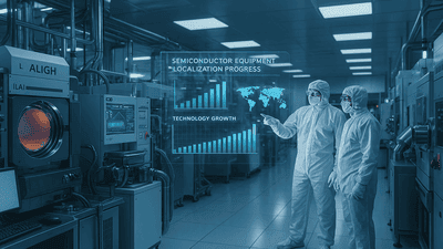
In the equipment domain, a 300B yuan fund could pursue several complementary strategies.
Scaling domestic champions. Identify existing domestic tool vendors with proven products and help them scale—through capital for new plants, R&D, and global outreach. This could be most effective in segments like etch, deposition, cleaning, and certain inspection and metrology tools, where technological barriers are high but not insurmountable.
Fostering new entrants in weak spots. Launch or support startups focused on gaps where domestic capability is thin: advanced packaging equipment, specialized test tools for high‑speed interfaces, or equipment tuned for compound semiconductor processes (e.g., gallium nitride, silicon carbide).
Co‑development with fabs. Use fund capital to encourage co‑development programs, where fabs and equipment vendors jointly optimize processes. This reduces risk for fabs adopting new domestic tools and accelerates learning cycles for vendors.
Export‑oriented equipment strategy. In areas not subject to export controls, domestic equipment firms can target international customers, turning Big Fund‑backed investments into future foreign revenue streams. Over time, this can shift China’s role from net importer to competitive supplier in select equipment categories.
Materials: building depth in the value chain
Materials investments are typically less visible than fab announcements, but they matter immensely in practice. Big Fund III’s capital could generate outsized benefits if applied strategically.
High‑purity production at scale. Semiconductor manufacturing demands extremely tight contamination control. Investing in plants that can meet leading fabs’ purity standards for gases, chemicals, and slurries is crucial. Even if some highest‑end materials remain imported, incremental improvement can close gaps and reduce vulnerability.
Advanced substrates and interposers. Modern packaging—especially for HBM and chiplet architectures—relies on advanced substrates and interposer technologies. Supporting domestic substrate makers and interposer fabrication capabilities would directly enhance China’s ability to build complex systems domestically.
Integration with research institutes. Materials often sit at the intersection of chemistry, physics, and process engineering. Big Fund III can catalyze collaboration between universities, national labs, and commercial producers, ensuring that new materials move quickly from lab to fab.
Qualification pipelines. Getting materials approved by major foundries and IDMs is a multi‑year process. Funding structured around qualification pipelines—shared test lines, pilot runs, reliability testing—can accelerate adoption and de‑risk materials for end users.
HBM and memory: targeted strategic depth

HBM has emerged as one of the most strategic memory technologies in the AI era. Its importance suggests that Big Fund III will treat HBM not as a generic DRAM category but as a system‑level capability.
Packaging‑centric HBM strategy. Given global constraints on leading‑edge DRAM IP and equipment, a pragmatic strategy is to focus on the packaging side of HBM. Investments might support:
- Facilities capable of reliable die stacking with TSVs at high yields.
- Thermal and mechanical solutions tailored to dense HBM stacks adjacent to high‑power accelerators.
- Test and burn‑in infrastructure tuned for HBM, where failure modes differ from standard DRAM packages.
Aligned accelerators. Big Fund III may encourage co‑development between domestic accelerator designers and memory producers. Matching HBM configurations to local compute architectures could produce competitive products even if absolute DRAM performance lags global leaders.
Gradual DRAM ladder‑climbing. Over a longer horizon, capital may support DRAM projects that climb technology nodes step by step, using domestic materials and partial equipment substitutions where possible. Big Fund backing can cushion the long payback times inherent in memory technology transitions.
Ecosystem risk‑management. Because HBM is tightly integrated into AI platforms, funding might be structured to spread risk across multiple firms, avoiding dependence on a single domestic memory champion.
Implications for China’s semiconductor trajectory
A 300B yuan Big Fund III that tilts toward equipment, materials, and HBM carries several long‑term implications for China’s semiconductor trajectory.
Reduced vulnerability at key choke points. Progress in domestic tools and materials lessens exposure to foreign export controls and supply disruptions. Even partial substitution can improve resilience and bargaining power.
Greater system‑level independence. Strength across equipment, consumables, memory, and packaging enables more of the system stack to be built domestically—from accelerators and HBM modules to full AI servers and industrial systems.
Competitive pressure on global suppliers. As Chinese equipment and materials firms improve, they may compete internationally in segments where they achieve parity or unique cost advantages. This could reshape global market shares over time.
Stronger local ecosystems. Regional clusters—combining fabs, OSATs, equipment vendors, materials producers, and research institutes—will likely deepen. Talent flows, supplier networks, and shared infrastructure will reinforce these ecosystems beyond the life of individual projects.
How global players should interpret and respond
International companies and policymakers will read Big Fund III’s moves as signals about future competitive dynamics. Several strategic responses are likely:
Global tool vendors. Non‑Chinese equipment suppliers may face rising competition in certain mid‑range segments over time. They might respond by focusing on cutting‑edge tools, deep service integration, and close partnerships with leading global fabs to maintain differentiation.
Materials suppliers. Foreign materials companies could see both opportunity and risk: opportunity in partnering with domestic Chinese producers or serving joint ventures, risk if local competitors gradually displace imports in some categories. Differentiation via performance, reliability, and co‑development support becomes more important.
Non‑Chinese chipmakers. Global foundries and IDMs will watch Chinese HBM and packaging capabilities closely. As domestic Chinese products improve, they may impact pricing and market share in regional AI and high‑performance segments, especially where regulatory or procurement policies favor local suppliers.
Policymakers elsewhere. Governments in other regions may see Big Fund III as a prompt to refine their own industrial strategies—whether by increasing transparency around subsidies, encouraging more open collaboration, or carefully calibrating export controls to avoid unintended technological fragmentation.
Risks and execution challenges
Even with 300B yuan at its disposal, Big Fund III will face significant challenges.
Capital allocation risk. Large funds risk misallocation—backing too many similar projects, overinvesting in technologies with limited commercial viability, or failing to cull under‑performing ventures. Strong governance and technical due diligence are essential.
Talent and know‑how constraints. Equipment, materials, and memory technologies rely heavily on specialized expertise. Scaling domestic capabilities is not only about money but also about experience and tacit knowledge that takes years to accumulate.
Global policy uncertainty. Future export control changes or geopolitical events could alter the viability of specific investment paths. Big Fund III must remain flexible enough to pivot as external conditions evolve.
Time‑to‑impact. Equipment and materials projects often have long gestation periods. The full impact of Big Fund III’s allocations may only become clear years after capital is deployed, making interim evaluation and adjustment important but difficult.
Conclusion: a deeper, more layered push into semiconductors
Big Fund III’s 300B yuan envelope signals a deeper, more layered push into semiconductors than earlier iterations focused primarily on wafer capacity. By emphasizing equipment, materials, and HBM, China is effectively targeting the “leverage points” in the chip ecosystem—places where progress unlocks broader capabilities across fabs, packaging houses, and system integrators.
For global industry participants, the likely outcome is a more complex competitive landscape: domestic Chinese capabilities will rise in selected tool and materials categories; system‑level independence will improve; and HBM‑plus‑accelerator ecosystems will increasingly have local variants. How quickly and effectively these ambitions are realized will depend on governance, talent, and global policy conditions—but the direction of travel is clear. The semiconductor race is no longer only about who has more wafers; it is about who controls the deepest layers of the stack, from equipment and materials to memory and packaging, and how intelligently capital is deployed to build that control.





